Just wanted to say I'll be in Berlin for a few days if anybody wants to say hi.
Lab is moving and I'm on the move, but I should also finally get settled and $$$ flowing in in the next few months, stand by for cool stuff.
Wednesday, December 29, 2010
Tuesday, November 30, 2010
Sulphuric acid decapsulation
Something I've been meaning to try for some time. Somewhat arbitrarily I decided to go analog, the victims were a 741 op amp and a 555 timer. The torture:
 The victim (I snapped the pins off since they are easy to remove and had more of an impact of nitric reactions):
 Initial setup:
 I didn't take a picture of this, but the solution started to turn brown and diffuse out around the IC before too long. Began to turn darker:
 And eventually black:
 The acid behaved differently in the 555 flask (misty, no creeping along sides in 555 vs creeping and no mist):
 After draining and some initial acetone rinse:
 The die is seen in the leftmost object. I've been told that sulphuric is useful for live decapsulation and it certainly shows here. Much of the "wiring" was preserved despite prolonged exposure to acid. Nitric on the other hand would have obliterated these. Not as visible, but also all of the bond wires were preserved.
Since they were both analog ICs made by ST, it less likely that they were different epoxies. Both used fresh acid. Probably due to some contamination in the flasks.
I'll try to update with some IC pictures. Nitric tends to leave a lot of residue. This on the other hand had overall clean dies, although one of them had sort of a grainy appearance, maybe from certain residues? Apparently the 555 didn't have a passivation layer and the 741 did which resulted in scratches on the 555 after I was careless during plucking and didn't realize it wasn't protected.
In summary, this is what I thought
Advantages
-Less fumes than nitric acid, MIGHT be safer with less equipment / ventilation. With the cover on my glassware and the top being somewhat cold from the environmental temperature, it seemed to reflux the acid and I didn't even really notice the fumes. Contrast with nitric where fumes are an inherent problem from the nitrate decomposition.
-Inexpensive
-Readily availible materials? Battery acid and drain cleaner are readily availible. Battery acid tends to be purer and would likely need to be distilled first, but drain cleaner (ex: Bull Dozer) is much stronger but with contaminants. In any case, generally not a controlled substance and one should be able to order it without too much trouble.
Disadvantages
-Higher working temperature. Might literally take your hand fall off if you spilled on it. When I was younger a single drop of cold concentrated sulphuric landed on my hand and caused a severe burn to which I'm reminded to this day by a scar. I can't imagine what a broken boiling beaker could do.
-From the solution turning black and the lack of bubbles, no clear indication of when its "done." Combined with the larger cool down time of the acid and glassware, this can make it inefficient for doing small batches.
Overall, probably a good compromise for those that want to try some of this stuff
-Grainy appearance on dies? Need to look more into what that came from
With this in mind, one good application might be to use it as a wash after nitric. Since I've found issues with particulate residues after nitric, a brief sulphuric bath might be able to clear them off. I think sulphuric works at lower (ie room) temperatures, albeit much slower, so it might not even require heating. I'll probably try to soak a fully encapsulated IC overnight and see how it goes as a starter.
Monday, November 8, 2010
Back to Troy, NY
After spending the summer in Cambridge, MA and back to SF Bay area for a few weeks, I've been back to Troy, NY. What makes Troy special? I'll tell you...
 Luxurious homes
 Expensive cars
 Booming industry
 And fine art
Okay, so its not quite as bad as I make it look, but most of these were taken pretty close to my apartment. To be fair, they've been knocking down a lot of the old buildings and graffiti is pretty rare except when this construction wall went up at RPI and people went nuts. I'll omit those pictures as if the first pictures don't get me hate mail, I get the feeling RPI might give me a "strong suggestion" to take down the latter.
Now that the small talk is out of the way, on to business. Although I haven't been posting anything, a lot has been happening. First, the microscope I previously mentioned never came, but eBay refunded me. However, my room-mate bought a metallurgical microscope with USB camera, so I'm better off than ever. Being off campus now, I also have less restrictions and don't have to deal with RA BS and such. One perk of my apartment is that I got some lab space in an area that's being remodelled. Its going to go away in January, but I'm hopefully moving out then anyway, so that shouldn't really effect me. The end effect of this is that I'm finally getting a chance to do all of the stuff I wanted to before and actually have some time and space to try things out.
I've imaged a bunch more IC pictures. In particular, I have images of discrete transistors, fully delayered 7404 hex-inverter, and other ICs.
 3906 top metal
 Old TMS320 logo section
On that note, a die image archive was started at http://intruded.net:8080/wiki/ Since I like Wiki's, I got myself an account and you should expect to see any die images I publicly release to appear there. I posted a few from a bit back, but haven't gone on a rampage yet. One of the things they are working on is getting a "Google Maps" style IC viewer for larger ICs. A crude test page is at http://intruded.net:8080/map/ (you'll have to zoom to correct level).
 Map view test for large ICs
Regarding http://siliconpr0n.wikispaces.com/, I recently got permission from Sergei P. Skorobogatov to include images from his Semi Invasive Attacks paper on the Wiki as long as they are credited to him. So, along with the other material I've been accumulating from my own research, expect some rapid expansion on the Wiki in the near future.
After delayering a few 7400 series ICs, I've realized I had in fact been at the transistor layer before, but just didn't understand what I was looking at. Probably bad been confused by all of the MOS pictures I had seen? In any case, I tried a 74163, but found it was too complex to start with. I could only recognize a handful of components. A few days ago I delayered a 7404 which should provide a much cleaner reference circuit since its small and more or less split into 6 regular units. Unfortunately, I let it sit for a while without agitating it, so it crystallized a bit, but should be fine for my purposes.
 7404 transistors
A quick overview of the techniques I currently use and why. Most ICs are in epoxy. I boil them in 70% nitric until the epoxy is removed. Lacking an ultrsonic cleaner, I wash them in room temp 3% HF for about a minute to clean the surface. This takes a thin layer off the top, which removes most debris. Then, depending on how patient I'm feeling, either room temperature or near boiling 3% HF to delayer the IC. If I want to keep it suitable for live analysis (mostly my roommate has been doing this), a Dremel "drill press" with a small endmill is used to make a cavity above the die. We use a rough estimate, usually slightly above the pins, to guess how far to go down. The package is pre-heated to 300F and a drop is put on top, allowed to etch, and washed with acetone before it dries out. Heating the acid doesn't seem to make a difference as its heat is negligible (plus transfer cool off) compared to many IC packages. I also played around briefly with another low cost method that is more automatic but less selective, I'll try to post something on that soon.
Finally, I'm interviewing with various companies and looking for a job, so if you think you might be interested in me, feel free to send me an e-mail at JohnDMcMaster gmail.com.
 Luxurious homes
 Expensive cars
 Booming industry
 And fine art
Now that the small talk is out of the way, on to business. Although I haven't been posting anything, a lot has been happening. First, the microscope I previously mentioned never came, but eBay refunded me. However, my room-mate bought a metallurgical microscope with USB camera, so I'm better off than ever. Being off campus now, I also have less restrictions and don't have to deal with RA BS and such. One perk of my apartment is that I got some lab space in an area that's being remodelled. Its going to go away in January, but I'm hopefully moving out then anyway, so that shouldn't really effect me. The end effect of this is that I'm finally getting a chance to do all of the stuff I wanted to before and actually have some time and space to try things out.
I've imaged a bunch more IC pictures. In particular, I have images of discrete transistors, fully delayered 7404 hex-inverter, and other ICs.
 3906 top metal
 Old TMS320 logo section
 Map view test for large ICs
After delayering a few 7400 series ICs, I've realized I had in fact been at the transistor layer before, but just didn't understand what I was looking at. Probably bad been confused by all of the MOS pictures I had seen? In any case, I tried a 74163, but found it was too complex to start with. I could only recognize a handful of components. A few days ago I delayered a 7404 which should provide a much cleaner reference circuit since its small and more or less split into 6 regular units. Unfortunately, I let it sit for a while without agitating it, so it crystallized a bit, but should be fine for my purposes.
Finally, I'm interviewing with various companies and looking for a job, so if you think you might be interested in me, feel free to send me an e-mail at JohnDMcMaster
Sunday, July 25, 2010
End of summer plans
As my summer internship comes to a close, I was never able to get access to microscopes over here. If i had bugged a large number of people I might have, but there was so much else to do in Boston that its just as well.
That doesn't mean that I haven't been preparing though. For starts, I've accumulated a small hoard of Intel CPUs that I will hope in the near future to image. The microscope I bought a bit back wasn't as good as I thought it was, although it should still be fine for short term work coming up. I'm very grateful to be able to borrow the microscope at RPI, but for a number of reasons it is good to get my own. After searching around for a large portion of the summer, a decent quality Olympus microscope showed up on eBay finally:
 What made this affordable? Two things. First, it was a first time eBay seller. Second, it coming from Thailand. So there's a bit of risk involved. Usually people don't scam on scientific items and if they do I can probably do a chargeback or possibly even a PayPal dispute. I'm not sure on their policies with other countries. If you scream loud enough, someone will usually do something if bad things happen.
The other part is I looked briefly into what it would take for me to order RFNA. From the companies I saw, they required you to be associated with a business. I'm not sure if I could play any tricks with my school, but from the business standpoint it would be very expensive. Yearly business registration fees seem to be pretty high in CA (something like $800 a year if I recall) which is not justified for this project.
Next, I've aquired some ground glass glassware, which has been on my TODO list since early high school. If I need to produce any chemicals for analysis now, it should be considerably easier and of higher quality.
I fly home for CA in two weeks. While there, my plan is to image a number of 7400 series logic chips to form a practical foundation. This should also be useful for others to study from. I could have bought some from Digikey etc, but I am thinking they probably use newer process technologies that would be harder to analyse. So, I heat gunned some off of old circuit boards and will be using those. Assuming those three weeks go well and my microscope arrives at RPI, as permitting during the school year I will start imaging the Intel chips.
Finally, I may be involved playing a small part in a commercial project coming up. While I will not be able to disclose the details of it, part of it would include them buying all of the acid and such I need to decap the chips, giving me an idea of how using commercial grade equipment contrasts. My role will be focused on the decapsulating and possibly aiding in the analysis.
Saturday, May 15, 2010
Biological, inverted microscope layer image comparison
Biological, top metal (220X):
 Biological interconnect doesn't image well as all black. Sample for comparison (not same area):
 If you are stuck with a biological microscope, set the intensity as high as you can and you should be able to make things out with your eye, but cameras might have more difficulty.
Inverted metallurgical (inverted), top metal (440X):
 Inverted metallurgical (inverted), interconnect (440X):
 Although all three are from the same chip type, only the two inverted images are from the exact same chip. NOTE: I have done a vertical flip on the inverted images to correct them to what the actual object is like (as in the biological image).
For those wondering where the magnification levels come from, it is a combination of the eyepiece, objective, and camera magnification. For the biological microscope, the image was shot at 10X eyepiece * 10X objective * 2.2X camera = 220X. For the inverted metallurgical microscope, the images were shot at 10X eyepiece * 20X objective * 2.2X camera = 440X. Thus, I (poorly) manually stitched two images together from each to get closer to the size of the biological image.
Alas, despite my best efforts, I still can't see transistors. Today I tried some extended hot baths in HF acid on the chip above and even tried adding some 30% H202 which dramatically increases the action of the HF. I'm letting it sit overnight (or maybe till Wed after finals) and see if it ate through. Maybe these chips are just resistant? I'll have to go back to sanding though to get other sample since I haven't gotten another technique to work yet on epoxied ICs.
Thursday, May 13, 2010
Image stitching
One of the challenges of using computer analysis is that it is highly desirable to assemble a full image of the chip, but only a small section of the chip can be imaged at a time.
For the DRAM example chip that's been used throughout several of these posts (its because they are easy to decap and I have a lot of them), I started by manually pushing the chip around since I didn't have linear stages and taking pictures, trying to get 1/3 or so overlap on each side. However, these initial sets resulted in far inferior results compared to those made by using linear stages. That said, I need to make a comparison where I manually paste the images together. In any case, I first tried to use Hugin to manually stitch the images together. Unfortunately, while Hugin works very well for standard images, it seems to have issues with the vectorized patterns typical of ICs. I was only able to paste two well formed pictures together after setting 15 or so control points:
 Thinking that I could do better, I looked into how to automate this process better. I cam across some information on the SIFT algorithm. Unfortunatly, while the SIFT algoirthm is patented by University of British Columbia, there are still some free implementations of it. The first I evaulated with autopano and later, after a reccomendation, was autostitch. Using the screwdriver pushed around die (as opposed to linear stage), with autopano, I go this:
 However, I can't find a result using the linear stage version. I need ot rerun on that to confirm that autopano can't do better.
Next I tried autostich. After some help from my friend on the linear stage set, I go this:
 My friend that reccomended it to me is a bit better at using it though, and was able to get a much nicer image seen here (warning: 16MB). Scaled down local version:
 His version is slightly more linear. My original image was quite distorted before he gave me the setting advice. In order to get good images with autostich, adjust quality settings to 100% (otherwise it will shrink it), set to linear, and adjust theta value low.
Inverted metallurgical microscope
A few weeks ago, Tom Ditto was kind enough to lend me this:
 A sample image:
 It has a number of differences over a standard biological microscope.
First, its primary advantage is that it does not require light to shine through the sample. Instead, light is injected directly into the view path, allowing easy view of opaque objects. I get around this with the biological microscope by shining intense lights to the side of the sample. I'm currently using a small 650W cone shaped halogen on a rheostat. Before I was using a 500W with a roll cage. I don't push it anywhere near full power. I had to make a shield to only allow in the needed amount of light and not toast the microscope with the intense heat it puts off.
Second, it inverts the image. As an example, here is an image of of an Intel 80486 ("486") copyright on the die:
 Note it is flipped. After cropping and inverting, a much nicer image is produced:
 Those black spots are dirt on the lenses. I've cleaned a lot off, but some of the larger spots are still present. In order to use this analytically, I will obviously have to fully clean it so spots of dirt don't appear where some critical interconnect image should be.
Various filters are available. I haven't played much with these though. I think the options include regular, polarized, and green. Here is a regular image, showing interconnect layers on some DRAM:
 With the green filter:
 Finally, although many do, for some reason the biological microscope I have doesn't have a movable stage on it. Maybe you were expected to push a slide around with your fingers? On the other hand, this one has an XY knobs for smooth, precise movement of the stage.
For future work, first on the TODO list is a proper camera mount. I'm using a clip on type mount that Tom let me borrow, but, unfortunately, its not stable enough for good images. This should fix alignment issues resulting in fuzzy, darker colors at the bottom and will allow me to zoom in, removing the dark circle. Next, I'm working on fitting some timing pulley's to the XY knobs for CNC control. I have all of the parts assembled for that and could probably due the fit in several hours. However, I need a larger peice of particle board to mount it on. Unfortunatly, I probably won't get back to this until August when I'm done working for the summer. With luck, I'll find someplace to continue work with it at MIT over the summer. Extra lab space anyone?
Why I'm not to the transistor layer yet, initial NaOH etch results
Several factors behind this. First, I'm approaching finals and haven't had a lot of time to delve into the deeper layers. Second, I haven't had much success in the few tries I've done to get below the metal layer. Although I should try this more, the initial sanding I tried with a dremel was too course. It had a tendency to produce a relativly uneven surface and take too much off. The HF would take off the top metal layer, but nothing else. I talked to Travis Goodspeed last night and he pointed out I should be (near) boiling the HF. Yum. Tried today briefly and I think I have some progress. However, I really need to take some pictures as I go to get a better idea of exactly what is being corroded.
I had also tried with some NaOH on a P3 die since I heard that is also corrosive to glass. I ordered some KOH which I read somewhere is preferred more in the semi industry, but it got sent to my home in CA by accident, so maybe I'll play with that in a few weeks. First, this is your typical P3 slot 1 die after being tin snip cut from the BGA carrier:
 This is actually a metalic blue, but apperas more black in the image. There is a gray epoxy holding it in place and a brown carrier around that. After inspecting the blue area under the microscope, I realized its just a coating to make heat dissipation better and not actually part of the silicon. In fact, you can see crystals poking through it (100X biological microscope):
 Unfortunatly, it was somewhat difficult to get a good picture of them, but you get the idea. Thinking this, being a large chunk of silicon, was a good canidate for NaOH etching, I boiled it in some NaOH for a bit. Result (note this is not the exact same chip as above):
 Hmm...what are those cracks? I think its stress from using the tin snips. If I was doing this for an imaging sample, I should probably dremel or carefully hacksaw cut them out. In any case, you can see the silicon crystalline surface much better (100X biological microscope):
 in this picture, one of the cracks is also visible. I'm actually not sure how much the NaOH etched the surface since I didn't realize the blue wasn't silicon and wasn't really paying attention to see otherwise. I'll try the other side of thise or some other dies I have laying around in the near future.
Also on the not going so well side, this is how my first attempt at a rosin decap ended:
 After ordering some borosilicate test tubes, I tried with a heat gun instead since I could control it with a variac and gave more regular results. After a few hours of boiling, a small nick came out of the underside of the chip along the die area, but not corroded as I was hoping. However, a large portion of this time was also devoted to boiling off the petrollium jelly after which the solution darkened and roes in temperature. The CCC IC RE Wiki page (written by Martin Schobert I think) shows the rosin doing more of a higher temp boil. I was at a lower boil. So, I might try to get a propane torch or a more proper alcohol lamp and try that. I'll have a few weeks soon to mess around at home and can probably figure something out. Also, this killed the TCO in the heat gun after I was done.
Tuesday, April 20, 2010
Paypal payload
There have been several advancements including work on finishing the automation of the biological microscope and automation of the inverted metelergical microscope, but school has kept me busy and I haven't had time to finish those. In the meantime, here is a small deviation on taking apart a security key to get to the IC. In such situations, there is a double decap. We not only have to decap the IC pacakge, but its a bit of an effort to even get to it.
At DEF CON 17, there was a side event of sorts called BSides/Neighborcon (thanks Travis!). This actually had my favorite talk of the entire trip by HD Moore on WarVOX. In any case, PayPal handed out stacks of the PayPal (or someone anyway, I think it was them) Security Key.

From some articles such as this it is based off of RSA’s Securid. I'm not a crypto guy, but I figure if I take some images of this and work out some of the logic, someone else more experienced in the field who can't do this type of hardware analysis might be able to build off of this work. I won't be be imaging the chip until I can get some more experience since future cards will cost me $5 a pop. Plus, I haven't made any agreements at this point not to tear it to shreds. I originally had a lot, but I gave them away to a number of people who thought they were cool.
One cool feature of these things its display Basically, it will retain the image on it even with power gone. It is the same (class?) of technology used in the more famous Amazon Kindle.
From what I hear, GM week at RPI use to be about getting wasted and they use to bring large amounts of beer for students to drink. But they don't do that anymore. I don't drink, but it would have been hillarious to watch. On the surface, its about elections...w/e. I still have my mug from last year which is better and I needed some glassware to dissolve the card in. To top it off, it had a Vegas theme, which seemed appropriete to make the card go full circle.
In any case, lets get started with the teardown. After a few minutes in acetone, the outter cover is starting to shed:
 A side view showing the ridges a bit better:
 I think peeled this off to speed things up and soaked it a bit more:
 The other half is starting to break apart a bit:
 A little dissolving later, I can peel off the outside plastic to reveal the circuit board:
 Closeup of the label section:
 There are very small surface mount components on the board. The label says "InCardIC006AV11". There's also a number 2, whatever that is for. My guess is that five dot gold pattern is for programming and/or testing. That black dot should be the IC, which is what I'm primarily after. Unfortunately, it has no external labeling of any kind. Finally, the last component is what appears to be a lithium polymer battery based on its shape. Voltage reading:
 Amazingly, the card still works! (the battery was removed later, still had battery here)
The acetone was getting a bit dirty. Time to clean it up a little:
 After soaking for the last time, I wasn't able to get much else to come off even after soaking for a while. I had been hoping the board was going to dissolve at least slightly and release the IC package. Final front board image:
 The battery came off with minimal force. Final back image:
 The black IC package was then forcably removed and stored into a vial for later analysis. As I get better suited to dissolve the resin, I'll dissolve it and take at least a top metal layer picture. In the meantime, I'll keep practicing on expendable chips so scarcer chips like this can be properly analyzed.
To top things off, what kind of person would I be if I let flammables go to waste?

At DEF CON 17, there was a side event of sorts called BSides/Neighborcon (thanks Travis!). This actually had my favorite talk of the entire trip by HD Moore on WarVOX. In any case, PayPal handed out stacks of the PayPal (or someone anyway, I think it was them) Security Key.

From some articles such as this it is based off of RSA’s Securid. I'm not a crypto guy, but I figure if I take some images of this and work out some of the logic, someone else more experienced in the field who can't do this type of hardware analysis might be able to build off of this work. I won't be be imaging the chip until I can get some more experience since future cards will cost me $5 a pop. Plus, I haven't made any agreements at this point not to tear it to shreds. I originally had a lot, but I gave them away to a number of people who thought they were cool.
One cool feature of these things its display Basically, it will retain the image on it even with power gone. It is the same (class?) of technology used in the more famous Amazon Kindle.
From what I hear, GM week at RPI use to be about getting wasted and they use to bring large amounts of beer for students to drink. But they don't do that anymore. I don't drink, but it would have been hillarious to watch. On the surface, its about elections...w/e. I still have my mug from last year which is better and I needed some glassware to dissolve the card in. To top it off, it had a Vegas theme, which seemed appropriete to make the card go full circle.
In any case, lets get started with the teardown. After a few minutes in acetone, the outter cover is starting to shed:
 A side view showing the ridges a bit better:
 I think peeled this off to speed things up and soaked it a bit more:
 The other half is starting to break apart a bit:
 A little dissolving later, I can peel off the outside plastic to reveal the circuit board:
 Closeup of the label section:
 There are very small surface mount components on the board. The label says "InCardIC006AV11". There's also a number 2, whatever that is for. My guess is that five dot gold pattern is for programming and/or testing. That black dot should be the IC, which is what I'm primarily after. Unfortunately, it has no external labeling of any kind. Finally, the last component is what appears to be a lithium polymer battery based on its shape. Voltage reading:
 Amazingly, the card still works! (the battery was removed later, still had battery here)
The acetone was getting a bit dirty. Time to clean it up a little:
 After soaking for the last time, I wasn't able to get much else to come off even after soaking for a while. I had been hoping the board was going to dissolve at least slightly and release the IC package. Final front board image:
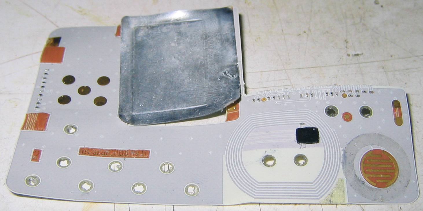 The battery came off with minimal force. Final back image:
 The black IC package was then forcably removed and stored into a vial for later analysis. As I get better suited to dissolve the resin, I'll dissolve it and take at least a top metal layer picture. In the meantime, I'll keep practicing on expendable chips so scarcer chips like this can be properly analyzed.
To top things off, what kind of person would I be if I let flammables go to waste?

Thursday, April 15, 2010
IC decapping round 4: burnt perfection
As you can hopefully see from some of the previous posts, people employ many techniques to remove the irritating resin casing. I've seen suggestions of simply burning away the casing, which I was somewhat skeptical of, thinking this would annihilate the chip. However, I am open to ideas, and thought I'd give it a spin.
First off, burning is probably a bad word. The image I had in my head of how this would work was the physically heat the chip until the resin was utterly destroyed, like burning away a piece of wood. It turns out its not hard to make the resin brittle through heating. Or in other words, all one has to do is apply a short burst of intense heat and you can crumble the casing away with minimal chip damage. A picture is worth a thousand words, lets see an example. This was the result of the first chip I tried:
 It came out amazingly clean like this in under a minute. Microscope inspection seems to indicate the die is healthy. More on this later. Starting from the beginning, here is a virgin chip:
 A CP82C59A interrupt controller. All torch images are of one of these, but not necesarily the exact same unit. A tube of them was being kicked around in the RPI Electronics Club junk drawer. Torch meat now:
 You shouldn't heat the chip too strongly. If you get this, you've gone too far:
 I actually would have never guessed you could get a red hot IC package. In any case, as will be seen in the video, the most important thing is even heating. I'm not sure what the shock temperature is, but there was a certain cutoff line where the chip was extremely brittle vs very hard. In the video I don't heat the lower half of the chip good enough and it only breaks moderately well.
After removing the torch, it will burn like a well down marshmallow for a few seconds:
 It should go out by itself fairly quick, but I was waving or blowing it out. Result:
 Breaking now:
 This final image is the die from the video. The one from the sequence above is the one on top shown here (contrasted with the very first one I flame decapped):
 The heat managed to separate the die and the carrier! So that's what happens when you apply too much heat. I wasn't paying attention at the time and I'm not sure what happened to the die. I figured it had been melted in some weird way where as it probably fell to the floor when I cracked the casing open. The first one I tried (bottom die above) couldn't have gone any better. The case split perfectly and no resin was left covering the die.
Seeing how well the die withstood the heat, I wondered how far can we go? So I torched a die red hot. Although it was not as clear under the microscope as before, it still was of decent quality. I'll try to add a pic in a bit comparing an area of the first die extracted with the one that I tortured.
Here is a short video showing an heat based extraction:
In this test setup, that blue thing is a filter system to help reduce fumes. I also have a gas mask handy for exactly this sort of work. It really does help a lot. The resin was really brittle and very little force was required to break it. However, I didn't heat it enough towards the bottom, so one side of the die was still relatively well set into the case. This can be easily fixed though and is partly due to me trying to get this on film and not doing for an ideal setup.
For some future work, I may have gotten away with this due to the relatively large traces the 2 um test die I used had. Thinner traces may be much more sensitive. Still, the results are much more promising than I was expecting. As I move down the semiconductor technology roadmap, I'll revisit this and see how well it does against finer masks.
Thanks to Will Carder for lending me the torch!
Subscribe to:
Posts (Atom)
