Tuesday, November 20, 2012

Speaking at EHSM


I'll be doing a talk on general IC RE techniques at EHSM in Berlin later December.  Come by and say hi!  (no I won't be wearing my super-villain outfit)  In other news, work has been busy so not many updates. But a few teasers.


Thanks to help from a friend or two I was able to write a reasonably working camera driver for my MU generation AmScope camera (MD is similar chipset but didn't have obscurified protocol).  Also CNC microscope software has undergone a revamp and is much cleaner and runs on Linux through gstreamer. Having the video widget integrated into the GUI is much more convenient.  I did a proof of concept run but haven't done any "real" imaging runs yet.


Additionally hardware is getting a revamp by adding CNC Z, theta X, and theta Y using picomotors.  If space permits I may add a rotary stage for manual (or possibly CNC) rotation.  This should allow nearly fully automatic imaging (the most time intensive part of imaging right now is leveling the chip).


Finally, I have been learning OpenCV and experimenting with automated techniques.  Needs work but I'm getting better and its been a good learning experience if nothing else.  In short, while Degate is out there I don't really understand how it works and can't improve it (at least the image processing side).  While degate focuses on standard cell matching I'm working with less regular older chips to form polygons.  So, it should form a good compliment to Degate as well as help me contribute as I learn more.

Sunday, July 1, 2012

ST 24C02 sector 17R (clock)

I'm going to post random parts of the ST circuit as I get to them.  For now here is what I'm calling "sector 17" (see wiki page for die location) right half.  I chose it because a quick glance showed some analog components, my guess was clocking related.

Here are the raw images with parts of the Independent/irrelevant left half taken out.

Top metal:


 Top metal removed (using hydrofluoric acid):


M1 removed (using hydrofluoric acid):


 Stripped to active areas (yet more hydrofluoric acid):


Converted using Inkscape with component and supply labels:


P1 and P2 is this circuits I/O.  Supply labels are from tracing from the power pads which I got from the 24C02 datasheet.  Alternatively you could trace from the PCB or recognize that PMOS tends to be larger than NMOS (note 2:1 contact ratio).  I'm not sure why the capacitors are isolated as they are all tied together in parallel.  Maybe some sort of DFM thing?  Unlink the other resistors which were smaller and resembled more of a depletion load design, this resistor (R3) is just a very long and narrowish active area.

Anyway, I then labeled every transistor, resistor, and capacitor so ease schematic capture.  Then I placed them in EESchema in rough layout order and finally wired together from reading the inkscape plot.  This yielded:


And then rearranging to be a little easier to read:

Now lets simplify a little.  We can now see that P2 is an input and P1 is an output.  P2 feeds into a standard CMOS inverter (Q22, Q8) which then feeds into a second CMOS inverter (Q21, Q7) to form a buffer circuit.  Similarly, Q17 and Q3 form an output inverter.  Going back to the buffer, its output feeds into an RC circuit.  Say the circuit starts with the capacitor bank (call it C) drained.  C will slowly charge as P2 is set to logic high and eventually reach a steady logic high condition. 

The next circuit is more interesting.  Lets start by taking a steady state approach to see what it does.  When logic 1 is presented as input we get the following:


An input of 1 turns on the two top NFETs (Q5, Q6) to conduct VSS to output.  The FET next to them (Q19, Q20) are P channel and so is off.  The PFET below (Q18) is switched on  but doesn't have anything to drive since Q19 and Q20 are off.  The circuit is complimentary so switch an input for 0 results in the same thing.  So far we have a really inefficient inverter.

But wait, there's more!  Lets see what happens in between.  Lets treat this as a discrete event simulator where each gate turns on in constant time.  Switching input to 0:

The old transistors are still on because the signal hasn't propagated yet.  Now take another simulation step: 


Now Q5 and Q6 are off and Q19 and Q20 are on.  And..oh dear...  In my computer hardware design class at RPI they showed us a similar circuit and told us that a designer that turns on both the N and the P channel at once is likely to get fired.  Are things so dire?  No.  First, notice that Q18, Q20, Q4, and Q5 are all a little bigger than the others.  Presumably thats so they can take this abuse.  Second, notice that this condition is very temporary.  In the nominal case Q10's gate will get drained a short time later with no new juince coming in and Q20 wins out in the end.  Alternatively, if the input goes back to 1 Q10 keeps the output low while Q5 and Q6 quickly switch back on.

So we have a device that preserves steady state and removes short pulses that swing in the opposite direction.  Such a device is called a Schmitt trigger.  I was able to verify this by finding this paper which had the following diagram:


Which looks exactly like this circuit.

Putting it all together we get the following:


More to come...

EDIT:
According to http://smithsonianchips.si.edu/ice/cd/STR98/EEPROM.PDF page 40, their similar ST chip says what I thought was M1 is actually poly (hey, its a learning exercise!).  I'll see if I can run some etch tests to confirm this.  A friend is working on doing a teardown of the EEPROM structure and I came across that while looking through previous work.  They don't go into gory detail though so he'll still do a writeup.

Thanks for the comments on the capacitors!  I'm working on a writeup of the charge pump so there are a lot more to come ;)

Saturday, June 30, 2012

Misc wiki pages

SRAM device teardown: http://siliconpr0n.org/wiki/doku.php?id=memory:sram

Capacitor example: http://siliconpr0n.org/wiki/doku.php?id=capacitor

Some other minor equipment info.

Also I'm working on a 24C02.  Browse around http://siliconpr0n.org/map/st/24c02/ for the raw images if you want to take a look. 

Also someone did a nice writeup on doing backside analysis: Functional Integrated Circuit Analysis I have an SWIR rated objective I was hoping to play around with something similar but it turned out to be less trivial than I hoped to remove the IR filter from my lamphouse.  I could buy another (an Olympus LH-50A if someone has one ;) ) but I haven't found one at a price I like.  I could just suspend the bulb but its a pain to align like that.

Sunday, June 10, 2012

Cold nitric acid experiments

70 % vs RFNA

As a sort of control I wanted to see if letting a chip in 70% does anything.  I'm not sure where these pictures went but the answer is no, not really.  I could still read the label on the 70% chip although the pins weren't visible anymore.

WFNA vs RFNA

H2SO4 is dirt cheap for me to get where as nitric tends to be expensive to the point where I actually distill my RFNA / WFNA.  I was distilling RFNA before but using it sparingly since it took a bit of work.  I've since realized that I can make WFNA much easier as the vacuum distillation is quite quick.  In fact, I did an experiment on some old (for emphasis, it may have decayed making this an unfair comparison) RFNA vs some new WFNA on the same chip which I let sit for 90 minutes cold.  Our prisoner assistant:


Each one was given 5 mL of acid and let sit for 90 minutes covered.  First look:


After washing (WFNA left, RFNA right):


Close up of the WFNA chip:


which even has some undercut (peeling from drying?) where as the RFNA was solid.

It seems that the fresh WFNA did a lot of damage where as the RFNA only did a little damage.  However, much close to when I freshly made the RFNA, I stored some in a polypropylene vial and it was severely eaten overnight where as I haven't noticed any degradation storing WFNA in the same vials.  Note that storing strong oxidizing mixtures in plastic vials isn't probably a good idea but it makes ultrasonically cleaning chips easier with what I have on hand.  I've been meaning to order some small PFA tubes but haven't gotten around to it.  Anyway, I wouldn't say that this is conclusive but my feeling is that at it is likely demonstrating that nitric decomposes significantly over time and should be used fresh.  Next time I make a batch of acid I'll make a batch of each and do a fresh comparison.

WFNA and H2SO4


The next thing I was curious about was that if H2SO4 could be used to enhance nitric acid cold.  I've noticed that nitric rapidly decreases in usefulness on epoxy with decreasing concentration.  My hope is that if I could dehydrate it with something it could prolong its life.  I've tried soaking some chips in cold H2SO4 and haven't seen any effects.  I've read that concentrated H2SO4 should cause the epoxy to swell but for one reason or another I haven't observed that (mines 98%, maybe not dry enough?). 

Our victims subjects:


2 Actel A1020B FPGAs selected for no particular reason other than that I had two of them.  I stripped off the outside pins from both before adding acid.  I added 3 mL WFNA in a PTFE beaker (an eBay seller had a bunch 3 for $5 so I bought a bunch of them) with a watchglass on top to one and 3 mL WFNA + 3 mL 98% H2SO4 to a PTFE beaker with a watchglass on top to the other.  This volume let both chips be completely covered at least at the start.  5 mL may have been a little better  I let them sit overnight, maybe 15 hours total.

WFNA

The WFNA initially etched very quickly as the solution turned dark after just a few minutes. The next day there was a lot of NO2 trapped:


Letting it air out:


Removing the acid:


Wash in water + ultrasonic clean in acetone:


The chip is only barely etched, maybe about 10% of the height (I didn't weigh them, maybe should have).  The Actel logo is even still a little visible above.  My first thought is that it may have spent most of its acid on the pins but there is exposed copper (after cleaning) at about the same level as the plastic package.

WFNA + H2SO4

This etched much slower than the WFNA.  In the few minutes after adding the chip where as the WFNA had turned very dark this was only tinted.  Letting it sit overnight had some NO2 but not nearly as much as the WFNA:


Draining the acid off:

A bit odd shaped.  The other side makes it look sorta like a rock:
Maybe this is what the H2SO4 swelling is suppose to look like.  It seems odd though that I wasn't able to observe it until diluting with another acid.  After cleaning it looked like this:


I'd say about 40% removal of the epoxy by height.

Conclusions

 Here are the washed + ultrasonically cleaned chips side by side (WFNA left, WFNA + H2SO4 right):


The WFNA chip turned red again but the other one didn't.  Presumably this is from acid residue and it would stay dark if I washed it more thoroughly.  Overall the WFNA + H2SO4 did pretty good.  It was slower but did well overall.  It had to be cleaned to figure out how far it actually etched (you can still read the Actel logo on it above!).  My guess is that the main reason it did better is because it didn't have to eat through the copper.  Failure analysis books recommend 10% H2SO4 + 90 % RFNA to passivate.  I'd have to do such a comparison to figure out if the excess H2SO4 did anything or if it simply helped by passivating the copper.  However, based on the swelling which I've never seen before, I'm going to guess that it had other beneficial effects.

The only thing that I was a bit hesitant about is that this is a very strong nitrating mixture.  MSDS say that nitric is incompatible with alcohols and acetone.  My experience has been that alcohols should be strongly avoided and that acetone is only a problem at higher temperatures.  However, I tried to mix a drop of each and it reacted violently instantly cold.  So in conclusion: this may be a good way to prolong acid when you are patient but the mixture must be treated with care.

For next time

I'm working on a teardown of a 24C02 EEPROM.  See top metal here: http://siliconpr0n.org/map/st/24c02__ns50xu/

Thursday, May 24, 2012

Interactive basic logic chip teardown


http://siliconpr0n.org/wiki/doku.php?id=quiz:metal_gate_cmos

When I first started I wanted to dissect a basic logic chip but the ones I looked at had funny power transistors and so didn't work well for getting my feet wet.  However, there are plenty that do use more standard MOSFETs and so here's one such chip presented as an interactive quiz.  Each quiz goes increasingly deeper into the chip and ends with explanations so that you can move onto the next level.  Its designed to either test yourself or as a learning exercise.  If you don't know the answers just make a best guess and you should get enough info at the scoring page to move onto the next quiz.  Enjoy!

Sunday, March 4, 2012

SiDoku #1

Flylogic gave a brief tutorial and a logic chip at http://www.flylogic.net/blog/?p=32 I have been messing with a standard cell based chip recently and this is one of the more complicated cells from it. In their spirit, here is a similar challenge.

Top metal (M1 and M2 visible):
Delayered:

Active area:

The two delayered images are "identical" but have different artifacts. I gave both since its what I used and it helps a little to piece things together. If you are the first to solve it and are interested I'll see if I can post at least a top metal photograph of a chip of your choosing. Get the chip to me somehow or if its something relatively common I might have it hoarded somewhere. Solving this means 1) giving a high level description of the functionality of the device and 2) A gate level schematic (ie with and gates etc where possible instead of transistors) with pins labeled to the M2 contacts

Hint: the two bridged contacts on the top metal (M2) are part of the cell and can assumed to be connected.

I'll release the solution in a week or two if no-one gets it. Some more resources to help including an inverter from the same chip: http://siliconpr0n.org/wiki/doku.php?id=cmos:start There are also some instructions on how to load these images into Inkscape at http://siliconpr0n.org/wiki/doku.php?id=tutorial:digitizing_with_inkscape

Monday, February 20, 2012

Silicon Pr0n (old) backup restored

I have restored the silicon pr0n wiki from an old backup so it should be less of a skeleton now. Find it here:
http://siliconpr0n.org/wiki/doku.php?id=start
It may be a bit rough around the edges still as a lot of things hadn't been polished up yet after the Wikispaces conversion

If you want to contribute send me a brief e-mail with your interests in IC RE and I'll create you an account.

Saturday, February 11, 2012

Tile stitch

Now that I have a microscope that can generate lots of imaging data stitching has become the bottleneck. I forget exactly how long but the large memory requirements of gigapixel (GP) sized images made it take a day or so to stitch on my desktop. I might have been fine with this except that something, I suspect enblend or one of its libraries, seems to generate a number of glitches when the images get very large. I've seen this on both 32 and 64 bit systems and should probably file a bug report... In any case, I wanted to reduce system requirements since I figured there was a way to do things better.

Recently I've been playing around with the Google maps API as an idea to use tiles instead of viewing the huge source images. I first played around and tiled a visual6502.org image, the MOS 6522 that you can find here. This is nice as people without powerful computers can view this large image at full detail. To be fair the jpg compression also significantly reduced its size although not to a point where significant quality was lost for my purposes. The tool to do this can be found here.

However, this still leaves the question of how to avoid creating the large intermediate images. After some thinking I came with the following:
  • nona (a "remapper": transforms source images to their location in the output image) will only output images that are in the cropped area. Note that it will still spend a small amount of time on each of the other images deciding if it needs to generate it
  • enblend (a "blender": resolves conflicts when two source images occupy the same area) output should only differ in areas where there's a potential conflict
  • There is no potential for conflict on areas where images are unique. In particular this is the edges and there is less conflict in the center 1/3 of my images since I have 1/3 overlap with neighbors
This allows the following algorithm.


Step 1: get an optimized .pto

You can get this from any source you want. I am using my pr0nstitch program (discussed in a previous post) which I then optimize for size and crop in Hugin. While the Hugin stage could probably be automated its at least doesn't take very long and gives me an idea of how well the optimize went before trying a full stitch.

For this example I'll show a smallish input image. When stitched with Hugin it looks like this:

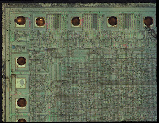
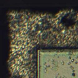
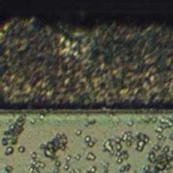
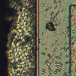
As an aside, this is a MOS 6522 that I used HF to remove the passivisation and then ate out the metal. Then end result is that you can still see where the metal was (because there is still a lot of SiO2 leftover) while still seeing all of the bottom layers.

Heres a visual from Hugin of what the input looks like:

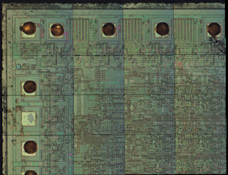
I think the color gradients are related to me using semi-polarized light on high quality but not strain free objectives (Mitutoyo plan apo 20X). On the bright side it makes the source image boundaries much more pronounced.

Step 2: pick the largest single panorama size you want to stitch


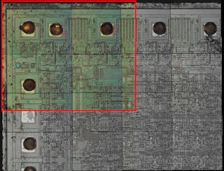
Ideally the supertile should be the largest size that enblend can fit into RAM (and is error free per the bugs I've had...). The software chooses 4X4 source image size by default (~2.5 X ~2.5 shown above) and has a command line option to customize.

Step 3: stitch the selected region


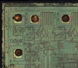
Remap (nona) and blend (enblend) to form a single large panorama image (a "supertile") that is a fraction of the entire output.


Step 4: generate tiles


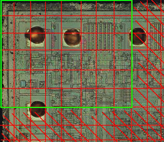
Greedy generate all tiles that are "safe" following the criteria from the last bullet above. I assume that images around the full panorama are fully safe as well as any images that are more than a half image width in from the border. Add these to a closed list as other supertiles may be able to regenerate them.

In the visual the red crosshatched areas represent areas that are considered unsafe because they are too close to an area where the blending could vary across supertiles. The green boxed in area are all tiles that we can safely generate. Here are a few actual tiles from that full sized image upper left hand corner:


Step 5: repeat for other supertiles

Shift the supertile such that you can generate more tiles safely. This works out to roughly shifting it by the border width + a tile size. Only generate the tile if its not in the closed list.


The tool can be found here.


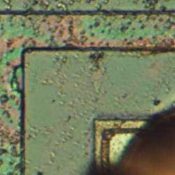
The first actual chip stitch I generated using this algorithm can be found here. There are a few stitching artifacts but I believe they are more related to bad optimization than the stitching process. I have been somewhat lazily always choosing the upper left hand image as the reference for position optimization. In several of my large stitches images get noticeably worse as you move away from this point. Additionally, there is a bug where I can lose a tile around the right and bottom. Presumably this isn't hard to fix as its probably something I need to just round up instead of down.

The performance improvement is also pretty good. I did several GP sized images and the stitch completes in about 3 hours. I haven't played with panotool's GPU mode to see if that results in any improvement. For reference my system has a 3 GHz Woodcrest dual core CPU (although I'm currently only using one) with 12 GB of RAM. I've been using a 10 GB enblend cache. On that note, I believe this algorithm could also be parallelized to one job per supertile without too much effort.

To be fair as part of this processed I also played around with caching options and such as I learned more about how the remapping and blending phase works. Things on the TODO list for next steps:
  • Fix the clipping bug
  • Start using a lens model
  • Try optimizing from a center anchor instead of a corner
  • Look into ways to improve the accuracy of the optimize step (ex: statistical deviations)
  • See what I'm losing by using jpg's over tif's / png's
Finally, my wiki Silicon Pr0n has been down for a while. Now that I have a job I decided to rent a VPS and get a domain name. The wiki is now at http://siliconpr0n.org/wiki/ This URL should now be stable regardless if the server blows up since I can always point it somewhere else. Additionally I have backups in place now. However, I'm still trying to recover some of the old data and it may have some (gaping) holes until I can get it back. I tended to post more material to that then this blog though so its a good resource to have back up.

EDIT:
For the heck of it I decided to figure out how to package this. Try it out at http://pypi.python.org/pypi/pr0ntools/1.0

Also I found that the anchor image for optimization is more important than I realized. A lot of my stitching artifacts appear to be due to my somewhat lazily choosing the upper left hand corner as the anchor which propagated a lot of errors. I'd still like to add a lens model though to see how that further improves error.