Here are the raw images with parts of the Independent/irrelevant left half taken out.
Top metal:
Top metal removed (using hydrofluoric acid):
M1 removed (using hydrofluoric acid):
Stripped to active areas (yet more hydrofluoric acid):
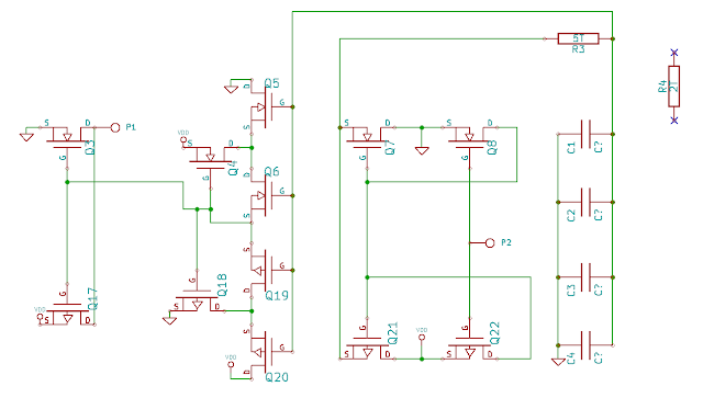
Converted using Inkscape with component and supply labels:
P1 and P2 is this circuits I/O. Supply labels are from tracing from the power pads which I got from the 24C02 datasheet. Alternatively you could trace from the PCB or recognize that PMOS tends to be larger than NMOS (note 2:1 contact ratio). I'm not sure why the capacitors are isolated as they are all tied together in parallel. Maybe some sort of DFM thing? Unlink the other resistors which were smaller and resembled more of a depletion load design, this resistor (R3) is just a very long and narrowish active area.
Anyway, I then labeled every transistor, resistor, and capacitor so ease schematic capture. Then I placed them in EESchema in rough layout order and finally wired together from reading the inkscape plot. This yielded:

And then rearranging to be a little easier to read:
Now lets simplify a little. We can now see that P2 is an input and P1 is an output. P2 feeds into a standard CMOS inverter (Q22, Q8) which then feeds into a second CMOS inverter (Q21, Q7) to form a buffer circuit. Similarly, Q17 and Q3 form an output inverter. Going back to the buffer, its output feeds into an RC circuit. Say the circuit starts with the capacitor bank (call it C) drained. C will slowly charge as P2 is set to logic high and eventually reach a steady logic high condition.
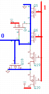
The next circuit is more interesting. Lets start by taking a steady state approach to see what it does. When logic 1 is presented as input we get the following:

An input of 1 turns on the two top NFETs (Q5, Q6) to conduct VSS to output. The FET next to them (Q19, Q20) are P channel and so is off. The PFET below (Q18) is switched on but doesn't have anything to drive since Q19 and Q20 are off. The circuit is complimentary so switch an input for 0 results in the same thing. So far we have a really inefficient inverter.
But wait, there's more! Lets see what happens in between. Lets treat this as a discrete event simulator where each gate turns on in constant time. Switching input to 0:
The old transistors are still on because the signal hasn't propagated yet. Now take another simulation step:
Now Q5 and Q6 are off and Q19 and Q20 are on. And..oh dear... In my computer hardware design class at RPI they showed us a similar circuit and told us that a designer that turns on both the N and the P channel at once is likely to get fired. Are things so dire? No. First, notice that Q18, Q20, Q4, and Q5 are all a little bigger than the others. Presumably thats so they can take this abuse. Second, notice that this condition is very temporary. In the nominal case Q10's gate will get drained a short time later with no new juince coming in and Q20 wins out in the end. Alternatively, if the input goes back to 1 Q10 keeps the output low while Q5 and Q6 quickly switch back on.
So we have a device that preserves steady state and removes short pulses that swing in the opposite direction. Such a device is called a Schmitt trigger. I was able to verify this by finding this paper which had the following diagram:
Which looks exactly like this circuit.
Putting it all together we get the following:
EDIT:
According to http://smithsonianchips.si.edu/ice/cd/STR98/EEPROM.PDF page 40, their similar ST chip says what I thought was M1 is actually poly (hey, its a learning exercise!). I'll see if I can run some etch tests to confirm this. A friend is working on doing a teardown of the EEPROM structure and I came across that while looking through previous work. They don't go into gory detail though so he'll still do a writeup.
Thanks for the comments on the capacitors! I'm working on a writeup of the charge pump so there are a lot more to come ;)


Loved it! You're in by bookmarks now. :D
ReplyDeleteCool project.
ReplyDeleteThe reason the capacitor is broken up is because of design rules. Large areas of metal create thermal stress or mess up polishing steps. Normally it's turned into a mesh, but in case of a capacitor you'd lose capacity and it's better to break it up.
FYI: if you want to find "exotic" µelectronics layouts hunt for mixed-signal chips. They're found where analog meats digital (e.g. ethernet chips) and they contain ESD structures and deep wells/isolation channels.
Another likely reason for the different sizes of the capacitor areas is to allow filtering of different frequencies of power supply noise. It is also sometimes recommended to use different value capacitors for power supply decoupling on PCBs (rather than mostly .1uF as is common) though I've rarely seen it put into practice.
ReplyDeleteOn the IC die the parasitic capacitance and inductance can be better controlled so it may be more practical / necessary to implement multi-band filtering like this.
Hi. Some comment about schematics. Q21, Q7, Q6, Q19, Q20, Q5 should have body connected to supply lines PMOSes to vdd and NMOSes to ground. I think it is not done in triple well technology. Output shmitt trigger together with inverter Q3/Q17 is non inverting one, which is weong on last schematic.
ReplyDeleteAny way it is nice to see this kind of projects.
Best Regards
Oops, definitely a mistake on the Q3/Q17. I couldn't find a non-inverting Schmitt trigger and forgot about it. Fixed.
DeleteRe: body connections I was admittedly somewhat sloppy with those and I mostly just grabbed the first MOSFET symbol I found in the library and didn't worry too much about it. I can certainly make some guesses like you did above, but it would be nice to stain the chip to actually see the wells (if I get time...). The charge pump I'm working on has some more interesting body semantics so that might be more anatomically correct.
It's good to see this information in your post, I was looking the same but there was not any proper resource, thanks now I have the link which I was looking for my research.
ReplyDeleteFlexible PCB
It's good to see this information in your post, I was looking the same but there was not any proper resource, thanks now I have the link which I was looking for my research.
ReplyDeleteMOKOPCB
Reply