Saturday, May 15, 2010

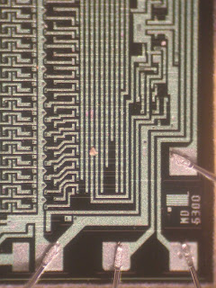
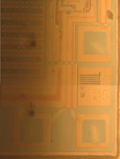
Biological, inverted microscope layer image comparison

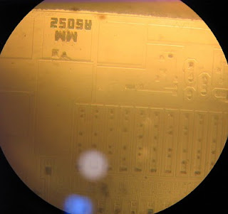
Biological, top metal (220X):
Biological interconnect doesn't image well as all black. Sample for comparison (not same area):
If you are stuck with a biological microscope, set the intensity as high as you can and you should be able to make things out with your eye, but cameras might have more difficulty.
Inverted metallurgical (inverted), top metal (440X):
Inverted metallurgical (inverted), interconnect (440X):
Although all three are from the same chip type, only the two inverted images are from the exact same chip. NOTE: I have done a vertical flip on the inverted images to correct them to what the actual object is like (as in the biological image).
For those wondering where the magnification levels come from, it is a combination of the eyepiece, objective, and camera magnification. For the biological microscope, the image was shot at 10X eyepiece * 10X objective * 2.2X camera = 220X. For the inverted metallurgical microscope, the images were shot at 10X eyepiece * 20X objective * 2.2X camera = 440X. Thus, I (poorly) manually stitched two images together from each to get closer to the size of the biological image.
Alas, despite my best efforts, I still can't see transistors. Today I tried some extended hot baths in HF acid on the chip above and even tried adding some 30% H202 which dramatically increases the action of the HF. I'm letting it sit overnight (or maybe till Wed after finals) and see if it ate through. Maybe these chips are just resistant? I'll have to go back to sanding though to get other sample since I haven't gotten another technique to work yet on epoxied ICs.

Thursday, May 13, 2010

Image stitching

One of the challenges of using computer analysis is that it is highly desirable to assemble a full image of the chip, but only a small section of the chip can be imaged at a time.
For the DRAM example chip that's been used throughout several of these posts (its because they are easy to decap and I have a lot of them), I started by manually pushing the chip around since I didn't have linear stages and taking pictures, trying to get 1/3 or so overlap on each side. However, these initial sets resulted in far inferior results compared to those made by using linear stages. That said, I need to make a comparison where I manually paste the images together. In any case, I first tried to use Hugin to manually stitch the images together. Unfortunately, while Hugin works very well for standard images, it seems to have issues with the vectorized patterns typical of ICs. I was only able to paste two well formed pictures together after setting 15 or so control points:
Thinking that I could do better, I looked into how to automate this process better. I cam across some information on the SIFT algorithm. Unfortunatly, while the SIFT algoirthm is patented by University of British Columbia, there are still some free implementations of it. The first I evaulated with autopano and later, after a reccomendation, was autostitch. Using the screwdriver pushed around die (as opposed to linear stage), with autopano, I go this:
However, I can't find a result using the linear stage version. I need ot rerun on that to confirm that autopano can't do better.
Next I tried autostich. After some help from my friend on the linear stage set, I go this:
My friend that reccomended it to me is a bit better at using it though, and was able to get a much nicer image seen here (warning: 16MB). Scaled down local version:
His version is slightly more linear. My original image was quite distorted before he gave me the setting advice. In order to get good images with autostich, adjust quality settings to 100% (otherwise it will shrink it), set to linear, and adjust theta value low.

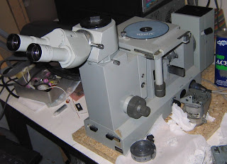
Inverted metallurgical microscope

A few weeks ago, Tom Ditto was kind enough to lend me this:
A sample image:
It has a number of differences over a standard biological microscope.
First, its primary advantage is that it does not require light to shine through the sample. Instead, light is injected directly into the view path, allowing easy view of opaque objects. I get around this with the biological microscope by shining intense lights to the side of the sample. I'm currently using a small 650W cone shaped halogen on a rheostat. Before I was using a 500W with a roll cage. I don't push it anywhere near full power. I had to make a shield to only allow in the needed amount of light and not toast the microscope with the intense heat it puts off.
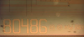
Second, it inverts the image. As an example, here is an image of of an Intel 80486 ("486") copyright on the die:
Note it is flipped. After cropping and inverting, a much nicer image is produced:
Those black spots are dirt on the lenses. I've cleaned a lot off, but some of the larger spots are still present. In order to use this analytically, I will obviously have to fully clean it so spots of dirt don't appear where some critical interconnect image should be.
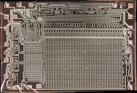
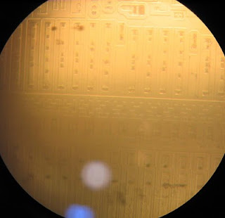
Various filters are available. I haven't played much with these though. I think the options include regular, polarized, and green. Here is a regular image, showing interconnect layers on some DRAM:
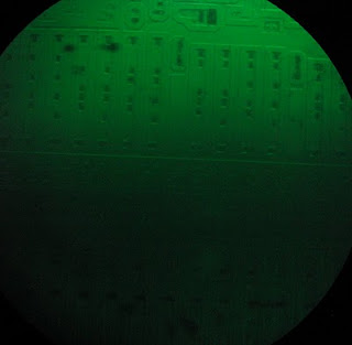
With the green filter:
Finally, although many do, for some reason the biological microscope I have doesn't have a movable stage on it. Maybe you were expected to push a slide around with your fingers? On the other hand, this one has an XY knobs for smooth, precise movement of the stage.
For future work, first on the TODO list is a proper camera mount. I'm using a clip on type mount that Tom let me borrow, but, unfortunately, its not stable enough for good images. This should fix alignment issues resulting in fuzzy, darker colors at the bottom and will allow me to zoom in, removing the dark circle. Next, I'm working on fitting some timing pulley's to the XY knobs for CNC control. I have all of the parts assembled for that and could probably due the fit in several hours. However, I need a larger peice of particle board to mount it on. Unfortunatly, I probably won't get back to this until August when I'm done working for the summer. With luck, I'll find someplace to continue work with it at MIT over the summer. Extra lab space anyone?

Why I'm not to the transistor layer yet, initial NaOH etch results

Several factors behind this. First, I'm approaching finals and haven't had a lot of time to delve into the deeper layers. Second, I haven't had much success in the few tries I've done to get below the metal layer. Although I should try this more, the initial sanding I tried with a dremel was too course. It had a tendency to produce a relativly uneven surface and take too much off. The HF would take off the top metal layer, but nothing else. I talked to Travis Goodspeed last night and he pointed out I should be (near) boiling the HF. Yum. Tried today briefly and I think I have some progress. However, I really need to take some pictures as I go to get a better idea of exactly what is being corroded.
I had also tried with some NaOH on a P3 die since I heard that is also corrosive to glass. I ordered some KOH which I read somewhere is preferred more in the semi industry, but it got sent to my home in CA by accident, so maybe I'll play with that in a few weeks. First, this is your typical P3 slot 1 die after being tin snip cut from the BGA carrier:
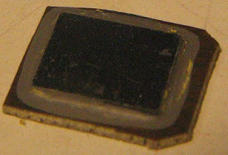
This is actually a metalic blue, but apperas more black in the image. There is a gray epoxy holding it in place and a brown carrier around that. After inspecting the blue area under the microscope, I realized its just a coating to make heat dissipation better and not actually part of the silicon. In fact, you can see crystals poking through it (100X biological microscope):
Unfortunatly, it was somewhat difficult to get a good picture of them, but you get the idea. Thinking this, being a large chunk of silicon, was a good canidate for NaOH etching, I boiled it in some NaOH for a bit. Result (note this is not the exact same chip as above):
Hmm...what are those cracks? I think its stress from using the tin snips. If I was doing this for an imaging sample, I should probably dremel or carefully hacksaw cut them out. In any case, you can see the silicon crystalline surface much better (100X biological microscope):
in this picture, one of the cracks is also visible. I'm actually not sure how much the NaOH etched the surface since I didn't realize the blue wasn't silicon and wasn't really paying attention to see otherwise. I'll try the other side of thise or some other dies I have laying around in the near future.
Also on the not going so well side, this is how my first attempt at a rosin decap ended:
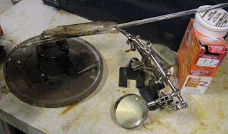
After ordering some borosilicate test tubes, I tried with a heat gun instead since I could control it with a variac and gave more regular results. After a few hours of boiling, a small nick came out of the underside of the chip along the die area, but not corroded as I was hoping. However, a large portion of this time was also devoted to boiling off the petrollium jelly after which the solution darkened and roes in temperature. The CCC IC RE Wiki page (written by Martin Schobert I think) shows the rosin doing more of a higher temp boil. I was at a lower boil. So, I might try to get a propane torch or a more proper alcohol lamp and try that. I'll have a few weeks soon to mess around at home and can probably figure something out. Also, this killed the TCO in the heat gun after I was done.