A bit of history first. This is the first IC capable microscope I got some time on:

But it wasn't well suited for computer control and inverted microscopes are difficult to mount IC samples in. I also got ahold of a biological microscope that could view ICs using a strong halogen light from the side. It did however have room to mount these:

The concept which you can kinda see here:

The mechanics were kinda iffy and worked so-so but it did get me thinking. After I got some money and with a little help I was able to get a Unitron microscope. Looking back it wasn't a super high quality microscope (very old?) but it got me a lot of experience to figure out what I needed. When I was about to scrap it I decided to get a little more aggressive with it and try to retrofit it for CNC control. It turned into this:

Which was finally a working CNC microscope! Very crude but I guess it turned out pretty well for the money and effort I put into it.
And here is the new setup:

Which cost me about 10X as much as the previous setup but is closer to the sort of thing I wouldn't want to run into in a dark alley or fear that might become sentient. It is interesting to note that the first run of this used the motor drivers and motors that the original setup failed to really get working. I only bought the linear stages for the original setup so I suppose the second setup cost about 10X as the original as well. An interesting progression of what you get for logarithmically increasing cost. I don't plan on adding a new point to that curve anytime soon ;)
Objectives
I was looking for several things for this:
- Mitutoyo objectives seem to be prized by many, wanted some to try out
- DIC seems to give good results
The DIC was a little trickier. I realized that the prisms aren't labeled very well and someone not very familiar with them might not know how to list them for maximum buck on eBay. So I kept an eye out for the two things that they might be attached to:
- Objectives
- Turrets

The whole assembly which I got for slightly more than a single prism sells for. Best of all they are nice Olympus Neo SPlan prisms as opposed to an older Neo prism. The set includes 10X, 20X, 50X, and 100X.
Unfortunately I didn't have any NIC objectives or polarizers. The real Olympus polarizers would easily cost me $300 for a pair surplus. However, I'm not sure how special the polarizers are or if you are really just paying for the mounts. So I bought a pair of polarizers for $8 shipped:
 Other side:
 Basically its 4 pieces:
- Polaroid (coated I presume) glass
- Aluminum case
- Retaining ring (screws in to hold the glass in place), visible in first picture
- Lose fitting outer ring, above writing in bottom picture
The section holding the lose fitting outer ring was milled out and it was discarded. This brings us to the device it will rest in. I found an old heatsink of the correct height and started shaping it a little closer:

Which was formed into this with the blank slider for comparison:
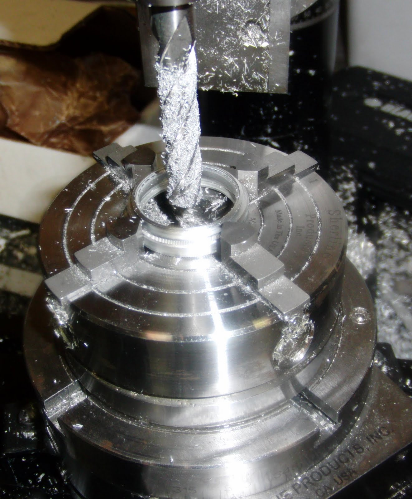
For several reasons I wanted the optic to be removable. The easiest way to do that tends to be to use a setscrew to hold it in place. Its a bad idea to put a metal setscrew directly against glass so I decided to use the aluminum case the polarizer came with to buffer the force. A setscrew holds the original polarizer case in the slider. The slider has a step in it so that the polarizer case can only be inserted from one side and holds things in place well. The optic is then inserted and the retaining ring holds it in place. It looks like this:

Which seems to have turned out pretty good. Fitting in the microscope:

And the matching polarizer is loosely sitting in the illuminator so that I can rotate it around:

I tried using a 20X Normarksi prism with a standard Neo SPlan 20X objective but it doesn't give you DIC so bit the bullet and bought a NIC rated one. I didn't get it at a super great price but wanted something to play with.
I also discovered that I had underestimated using polarized microscopy. You can get a number of really neat effects on semiconductors by using crossed polarizers. I think my cheap polarizers give a dark purple-blue color when crossed but I like blue so it turns out okay. I'm glad to have a reasonably high power lamp as this takes considerably more light than standard brightfield microscopy.
XY / linear stages hardware

The core of the robotics section are two Micro-Controle / Klinger / Newport high precision stages. They were listed as being from a high precision milling machine or something. This could be the case as while most stages are direct drive motor to shaft these have a planetary gearbox:

This increase their torque (which I really don't need) but it also makes it easier to move smaller distances. I'm not sure what the actual precision of the stage is but the aggregate step size I get out of the system is about 110 nm. So far this has been far above anything i've needed but it may become more convenient as I move to 100X imaging.
For whatever reason they use variable reluctance motors which I'm unfortunately not as familiar with as stepper motors. I tried making a simple stepper like driver for it but it couldn't hold up under any reasonable load. I read some papers and ultimately decided it was going to be less work for me to adapt some stepper motors on it.
The two drive motors are two slightly mismatched NMB brand NEMA 17 motors. I selected NMB motors since I was hoping that they would use the same connectors as my NEMA 23 Sherline motors but no dice. Even so it has been really nice that the motors have plugs that allow me to quickly disconnect the wires. They are mounted to the stages via some cheap flexible shaft couplers. I had to make some shims to get the 1/8" (0.125") Klinger motor shafts to fit into the ~0.2 NEMA 17 shaft couplers. Note that I didn't remove the motor as it contained the sun gear but rather replaced the opto-encoder disc at the end:

I machined them out of some old steel standoffs by carefully turning them on a rotary table and using a 1/16" endmill to mill out the center. To be honest I was quite surprised I didn't break the endmill. The adapters would have worked really well except that they deform when clamped and so it wasn't a good idea to try to move them around. Things still work okay but I might want to try to make some fresh shims or order some brass rod for a more proper solution.
Robotics electronics
All three motors are driven by Precision Motion Controls stepper drivers. These are fed by a "USBIO" PIC based microcontroller board. Basically I hammer on some GPIOs through USB. On my Linux machine I was able to get some MHz but the Windows machine this runs on seems to be limited to about 500 kHz. I'm pretty sure the motors can move a lot faster than this but it would take more care in software to try to get velocity and acceleration matched well enough so that things don't slip. Since Windows XP isn't exactly an RTOS I'd be surprised if that could be made super reliable but possibly well enough for what I need.
Unfortunately while the USBIO board is powered off of a 5V USB line it uses 3.3V logic. Logical 1 is defined as > 3.5V on my motor units which was causing unstable control. To solve this I added a simple buffer chip powered off of the USBIO board's VCC breakout:

The buffer chip (a CD4069 or something, I forget which exactly) doesn't actually give near 5V out but its good enough for what I need. I couldn't find any industrial style (ie with screw terminal) voltage level converters but I assume they must exist. Its not a terribly complicated circuit board, maybe I'll make some to clean this up a little. I have some perf board laying around which would also probably do the job.
Control software
The software is descended from the original control software. However, its very different in that it performs control in realtime instead of generating g-code. Its at roughly the same location as the original software, I'll probably merge it into the original's location one dir up but until then you can find it here..
I tried a few different imaging libraries and eventually settled on the Python Imaging Library (PIL). Although I had used PIL before for image processing I didn't realize it could do image capture as well. It has mostly worked well but I have gotten truncated images on a few imaging run. I think it may have losely had to do with AmScope software fighting with my software and so I added a check to refuse to start a job if the AmScope software is running.
The USB device has a serial driver so no real magic there. I did write a wrapper class but I already had that from previous projects.
After a little thought I decided I wanted a GUI to make moving around more freestyle instead of entering coordinates at the command line. Most of my GUI experience is using Qt so PyQt seemed like a good choice. Its a "programmers GUI" in the respect that its a jumble of UI components without much thought to ergonomic / careful placement.
The old setup used a point and shoot with mixed results. It was nice that it could auto-focus but it was bad that it would sometimes focus poorly and that I couldn't decided what I wanted to focus on. So I decided to look around for a real microscope camera and found a AmScope MD1800 (8.1 MP USB) at a halfway decent price.
Originally I was using the camera through the eyepiece but this had several issues:
- Tended to move around
- Couldn't look through very easily

I attempted to reverse engineer the camera driver to get it working on Linux and kind of got it working except that I haven't figured out how to sync frames. I'll see if I can post some of the data dumps here in case someone has an idea as I'd love to ditch Windows.
Focusing
On the old microscope the sample rested on a kinematic mirror mount (not shown) which allowed basic sample adjustment:

However, this was on a boom so it was difficult to adjust without shaking things around. However, I was able to compensate a little as the main reason that it was mounted that way was so that I had focus control from a precision Z stage. This allowed to compensate a little but didn't solve the fundamental problem. Also, the Z axis was kinda shaky and held in place by a rubber band to keep backlash down (the spectrometer it was scrapped from had the mirror weight holding it down). So for the second revision I tried to improve both of these focusing elements which I'll describe separately.
Active focusing (z axis)
I focused (haha) on this first since its what I used on the old setup. Z axis control is via a NEMA 23 motor with a timing belt coupled to the fine focus knob:

After taking the focus knob cover's off I noticed some threaded rod was sticking out:

Its probably M6 but I don't really know for sure. I had a timing pulley on a 1/4-20 bearing. This sounds like a really bad idea at first since the thread doesn't match and it would just slip around anyway. However, neither of these is hard to get around. 1/4-20 is very similar but not similar enough to mount directly on. Fortunately I had an M6 standoff that fits well on the microscope and that the 1/4-20 screws into pretty well too. Finally, I put a serrated washer between the pulley and the spacer to fix it in place.
Most of my pulleys are designed to fit NEMA 23 / 0.25" shafts which was part of the reason why I wanted to use a NEMA 23 motor. So, mounting that drive pulley was easy. I'm trying to avoid mounting the motor on the microscope in hopes of trying to reduce vibrations and so its currently mounted to the adjacent optics table via 1" 80/20 t-slot aluminum. I have to re-adjust it every time I move the course Z axis but its not difficult to adjust. I've considered several alternatives (attach with damping to microscope, rail mounted, etc) but haven't settled on something more permanent yet, in part because I'm not using this much as described next.
Finally, this has considerably more vibration than the XY motors which makes me less enthusiastic to use it. I'm not sure if its because the micro-stepping isn't adjusted properly on the NEMA 23 or just that it tends to move around more than the smaller NEMA 17 XY motors. I slowed it down a lot more than the XY motors so that its at a reasonable level but I'm pretty sure the mechanics could be improved.
Sample leveling
I also wanted to improve the basic angular control. It would have been nice to have this under computer control but, since its a one time (per sample or sometimes per multiple sample run) setup thing, its not a high priority.

Theory
This is how our system might look to an observer:

The line at the bottom represents the focal plan para-axial with the objective. The pivot is the bearing on which the kinematic mirror mount mirror holder rests. Turning the screw at the end raises or lowers the end of the plate in a single axis and effectively controls a single angle. We are only interested in the top of the sample and not the mirror holder that the sample rests on. I assume the sample is flat such that its surface forms a focal plane. The second line represents some adjustment of the axis screw to form a second focal plane.
Note that this model assumes that the XY plane is still parallel to the imaging plane. This is a non-trivial assumption since this difference is likely to be signifigant and result in requiring active Z focusing to get a good image. However, for my purposes the most important thing was to level out samples like packaged chips that may need significant adjustment. My stages are reasonably precise but I have yet to determine if I need to try to level them out better. The easiest way to do that is probably to insert shims or play around with how tight I set it in. The bottom stage only has 1 out of 4 screws installed and is probably the largest source of imperfections. I have been considering either drilling out the original plate or creating a new one so that it can be secured more regularly.
In this system angles are relatively small, hopefully no more than a few degrees. This allows us to make a small angle approximation so that sin(x) ~= x to simplify the math. This gives a triangle:

The following ar proportional:
a / a' : (t + t') / t' : (z + z') / z'
a / a' = (z + z') / z'
We know a, a', and z and want to find z'
z' a / a' = z + z'
z'( a / a' - 1) = z
z' = z / ( a / a' - 1)
Taking a few simple cases to get a warm fuzzy feeling this is correct. The two simple cases are that the first angle was correct and that the second angle was correct.
If the first angle was correct:
a = 0
z' = z / (0 / a' - 1) = z / (0 - 1) = -z
That is we have to go back to where we were originally
If the second angle was correct:
a' = 0
z' = z / ( a / 0 - 1) = z / (inf - 1) = z / inf = 0
That is we stay where we are.
Practice
In practice this above turns out to be too cumbersome to do by hand. If I had computer controlled tilt capabilities (such as with a Newport / New Focus 8071) these formulas might be more directly useful. I tried to apply them and the time to whip out a calculator and try to turn the knobs "just right" doesn't work well enough.
However, you can observe that if you iteratively do the following:
- Focus on a point close to the pivot, ideally the edge of the chip is on it
- Move to a distant point on a single axis, ideally the other edge of the chip
- Adjust the screw until in focus
- Move back to original location. If its still sufficiently focused you are done with this axis
- Repeat for the other axis
I'm thinking of marking some guidelines on the stage to make placing chips at the pivot point easier as this is theoretically just a single pass when that's the case. If they are not at the origin it will take more passes but typically not more than 4. For a large chip such as some GPUs I've been imaging my stages are slow enough that it can take 2 minutes to reach the other side. So, for these chips its taking about 20 minutes to level. Its not so bad though since the manual interaction doesn't take very long. (update: I did scribe some lines, was a very good idea and chip placement is much quicker now)
Ultimately this seems sufficient without any active Z control. On this setup the stages seem para-axial enough to the focal plane that I don't require any active focusing control. Since using an active Z axis still doesn't eliminate uneven focusing across an image this method is generally preferable. Currently the main advantage of the active Z control, although I'm not using it much anymore, is that it reduces setup time since it only requires collecting three or four points in a fairly small timeframe.
Next steps
I fed some images into the stitching software I was using before and they come out a lot better because of the closer to planar setup. I played briefly with constructing a more proper lens model and it would be a good idea to give that another go.
I'd like to share the chip images but I'm realizing they more or less take up obscene amounts of bandwidth and storage. I briefly played around with a Google maps style display but didn't pursue it very heavily as it may at least cut down bandwidth and relieve the burden of needing to open huge image files.
I played around with some focus stacking but wasn't terribly impressed. I need to see if I can find some more fine tuned options in panotools or look into alternative software. This is a real problem at higher resolutions (ex: 50X) on large chips where there may be many layers. If I only store the final focus stacked images I don't lose much disk space or imaging time and the pictures in theory can look a lot better.
Somewhat unrelated and on my TODO list is to finish digitizing the MOS 6522. I put a lot of work into getting a better imaging platform and I'm now getting pretty satisfied that I do. I want to focus future work on acquiring data and automating analysis. My first goal is to try to find techniques for automatically extracting the metal layer. Among image processing techniques I'm thinking of trying to use IR light since everything else should be pretty transparent to it. However, there are a large number of minor difficulties to get this to work so I may try visible techniques first. One thing in particular is that metal tends to saturate the video sensor without any polarization which I could probably use to my advantage.
I'd like to be able to rotate samples easier and install my larger and flat kinematic stage. The easiest way for me to do that is to remove the bottom illumination lamp housing / stand and replace it with my Newport rotary stage and a riser plate. I'm looking to see if I can get a precision lab jack like a Newport 281 but they look like they cost more than I want to spend. However, I've already had some commercial interest in some people wanting to use this system for wafer failure analysis imaging and so it might be worth the investment as it would allow me to image wafers a lot easier.
Finally, I'd like to improve the motor mounts so they are wiggle free. This shouldn't be too hard as I either just need to spend some time on a lathe (I don't have one but I have a Tech Shop membership) or to order some telescoping brass tubing and fit as needed. While this doesn't seem to effect imaging too much I'm sure its not ideal on the motors and probably causes friction that could effect repeatability, especially if I want to raise speeds.


