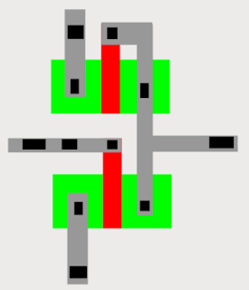
This post builds on a previous post where I described how to manually build a NMOS clock driven inverter in JSSim. It gave this (see it live):

I concluded by saying I was going to look into automating it and here's the first cut. I tried poking around for tools to automatically convert image files to JSSim files. They seem to either be not fully automated, don't exist, or are squirrelled away somewhere where I can't get to them.
The squireling possibility comes from that I would find it hard to believe that someone actually typed up all of the content in the *.js files. They are difficult to read as is (polygons are position dependent x/y coordinates in a long array) and it seems it would be error prone and tedious to generate that much data from the image files. That said, it did take them a large number of hours to complete the 6502 and it may not have been worth it.
Quietust wrote a toolchain more recently that you can find at here (my sandbox copy on Github). Since it only appeared recently it could not have been used to generate the 6502 meaning there is still a missing link even if there is an alternate route. I messed with it briefly and could not get it to parse my input SVG files. I've since learned more about SVG and probably will have a better idea of why it couldn't parse them (SVG is a huge specification, can specify a rectangle as a rectangle, polygon, patch ,etc), .
Finally, the first point that they are not fully automated comes from the fact that FPGA-netlist-tools. This toolchain is centered around producing synthesizable HDL from a variety of sources (images, JSSim). It has some good tools that pull in a lot of support from Magic VLSI, KLayout, Icarus Verilog, potrace, ImageMagick, gdspy, scipy/ndimage, and more. For example, I was impressed with how little code masks_to_netlists.py (136 lines including comments) used to create netlists from chip images. I was told that it may be possible to convert the output into JSSim files but haven't thoroughly explored it yet. It might not be too much work but I do need to learn more about various EDA CAD formats (CIF, GDS, spice, tech, etc) to figure out what I need to do.
Ultimately I decided I'd rather see how hard it is for me to do it with what I had available and then add support, rework, and integrate with the other tools as I learn more about them. I probably learned a lot more about for example, SVG format this way than I would have by blindly using the other tools/libraries.
For my test case I started by redrawing my image in Inkscape:

after deciding SVG would be easier than a raster image (ex: .tif) to parse. I tried a few conversion utilities with the following results:
- Open .tif in Inkscape and save as .svg: .tif embedded in .svg, not useful
- Convert using ImageMagick "convert" utility: created an element for every (non-white?) pixel. Impractical
In order to convert an image into decent JSSim code you need to do the following:
- Render polygons to screen in correct layer in correct net
- Figure out net connections: which components are connected
- Identify transistors
- Identify pullup resistors
- Identify net names for inputs (and potentially outputs too)
- Provide transistor geometry. Its used to find transistors which isn't used in main simulation
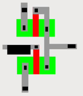
Rendering the polygons is fairly straightforward input to output conversion. After a small bit of research I decided to use Shapely's libgeos GIS library Python bindings for polygons. My simple SVG files were only rectangle, so I only had to parse rectangles. My core engine is built on polygons though and does work with them as demonstrated by the fact that I was able to merge rectangles into single polygons. However, since I drew the polygons as rectangles, I had to combine them. Otherwise you get results like this:

The alpha transparency on the metal doesn't overlay well and shows the underlying construction. I eliminated this by simply using a polygon union function on intersecting polygons on the same layer, replacing one of the polygons, and removing the other. You may also observe the image is upside down. SVG uses an upper left coordinate system and JSSim uses a lower left which means final conversion requires a horizontal flip.
Nets were decided by first assigning each node to a net. I then merged nets when one of the following happened:
- A polygon intersected itself on the same layer
- A via intersected diffusion, poly, or metal
I thought transistors were going to be difficult to identify but it turned out to be rather simple at least for this simple case. Transistors occur when two diffusion regions are separated by a poly gate (or metal gate for old school CMOS, but uncommon and not supported right now). I expanded each diffusion and poly polygon around its center of mass by a few pixels to find near neighbors and plotted the intersection (plotted using Tkinter):

I'm not sure how this method will scale but will see as I try it out on actual chips. In particular it will only accept the match if there are two intersections but I could easily imagine two gates being controlled by the same poly segment. I'll have to add some arbitration logic to sort out the connections if/when that becomes an issue. With two diffusion nets and a polygon net, we now have the two connections and the gate nodes respectively. I'm currently using the entire poly segment as a rough approximation of where the transistors is but maybe a better approach would be to try to protect between the two intersection polygons.
Pull-ups aren't that hard to identify once the transistors are identified. A pull-up requires the following:
- One connection to positive voltage / VDD
- Other two connections shorted together
Finally we have to identify the net names for input and output so that we can actually play with the chip. FPGA-netlist-tools specifies node names as a text file with the various coordinates and names specified in the file. However, I figured I could take advantage of SVG's being able to store text and place that information directly in the layers. From a conceptual standpoint I look for the intersection of the textbox polygon with a net and label that net which is similar to the point concept. This seems fair to do for the following reasons:
- Most important signals are on the pads which typically don't have wires running under them in a non-flip chip padframe
- Current chips don't have enough layers that they can't be unambiguously identified. In theory a very dense chip could have multiple metal layers that make resolving which layer we refer to ambiguous
- Could potentially allow layer specific labels if there were collisions which would allow unambiguous identification. Alternatively could put some markup in the name such it gets identified. For example, instead of "clk0" put "metal2:clk0" to say that clk0 belongs to metal2 which would otherwise be ambiguous

You have to careful though since text boxes can be much larger than the text. For example:

If this box was any bigger it would have hit diffusion and caused issues.
When the tool runs it looks for layer files in the current directory and spits out *.js. Running in JSSim (see it live):

We now have straight polygons! Mostly anyway. Zooming in:

In particular you'll notice this since it makes segdefs.js larger with the extra 2 points we added. If you look back at the non-merged metal it should be pretty obvious where this comes from. If I care to remove this I'll have to implement some sort of smoothing function to remove points close to each other.
My next step is to try to convert some of the chips in FPGA-netlist-tools into JSSim chips. I believe polygon intersection is somewhat computationally expensive and may have to implement a quadtree map for efficient large scale operation.
Until next time.

No comments:
Post a Comment