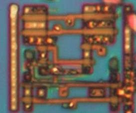
Top metal (M1 and M2 visible):
 Delayered:
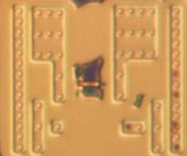
 Active area:
The two delayered images are "identical" but have different artifacts. I gave both since its what I used and it helps a little to piece things together. If you are the first to solve it and are interested I'll see if I can post at least a top metal photograph of a chip of your choosing. Get the chip to me somehow or if its something relatively common I might have it hoarded somewhere. Solving this means 1) giving a high level description of the functionality of the device and 2) A gate level schematic (ie with and gates etc where possible instead of transistors) with pins labeled to the M2 contacts
Hint: the two bridged contacts on the top metal (M2) are part of the cell and can assumed to be connected.
I'll release the solution in a week or two if no-one gets it. Some more resources to help including an inverter from the same chip: http://siliconpr0n.org/wiki/doku.php?id=cmos:start There are also some instructions on how to load these images into Inkscape at http://siliconpr0n.org/wiki/doku.php?id=tutorial:digitizing_with_inkscape
Here's my guess:
ReplyDeleteIt's a 1-bit latch with inverting and non-inverting outputs.
I've made a drawing at http://vogel.cx/sidoku .
Wow, I didn't expect anyone to *read* this that fast let alone solve it. I'll have to find something harder next time. Yes, that is correct. Originally when I was trying to decoded this I made the bad assumption that M2 wasn't part of the cell. Have a chip of interest? :)
DeleteYes, actually, I have. Can you send me an email at vogelchr at vogel dot cx to discuss the details?
DeleteMy official solution disagrees with yours as to Vdd and Vss. Yours has ground on the right side but mine has it on the left. This of course results in Q and Q# changing place and the clock/enable line changing from active high to active low.
ReplyDeleteMy version is based purely on the active-area image in which the transistors on the right side are PMOS, which are presumably connected to the power rail. Did you make a mistake or did you see something we missed in our analysis?
In any case you're pretty much correct. Here's my tracing, rotated into canonical orientation (Vdd rail at top): http://colossus.cs.rpi.edu/~azonenberg/downloads/cell07_traced.jpg
That's the beauty of CMOS :-) But Q and Q# don't change, if you think about it. It's only E vs. E#.
Delete