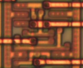
Top metal (M1 and M2 visible):
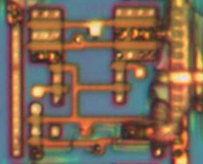
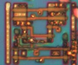
 Delayered:
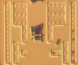
 Active area:
The two delayered images are "identical" but have different artifacts. I gave both since its what I used and it helps a little to piece things together. If you are the first to solve it and are interested I'll see if I can post at least a top metal photograph of a chip of your choosing. Get the chip to me somehow or if its something relatively common I might have it hoarded somewhere. Solving this means 1) giving a high level description of the functionality of the device and 2) A gate level schematic (ie with and gates etc where possible instead of transistors) with pins labeled to the M2 contacts
Hint: the two bridged contacts on the top metal (M2) are part of the cell and can assumed to be connected.
I'll release the solution in a week or two if no-one gets it. Some more resources to help including an inverter from the same chip: http://siliconpr0n.org/wiki/doku.php?id=cmos:start There are also some instructions on how to load these images into Inkscape at http://siliconpr0n.org/wiki/doku.php?id=tutorial:digitizing_with_inkscape
